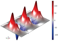
Plasmonic Waveguide Analysis
Surface Plasmons (SP) or Surface Plasmon Polaritons (SPP) are electromagnetic excitations that propagate at the interface between a dielectric and a conductor, and are evanescently confined in the perpendicular direction to the propagation. They arise via coupling of the electromagnetic field to oscillations of the conductor’s electron plasma and are characterized in terms of dispersion and spatial profile. From an electrodynamic view, SPs are a particular case of a surface wave: from the optics view, SPs are optical modes of an interface: from the solid-state physics view, SPs are collective excitation of electrons. The behavior of Surface Plasmons can be described by Maxwell’s equations as long as the properties of metals at optical frequencies can be obtained from experiment or theoretically calculated from the Drude model of electron conduction.
Surface plasmonic waveguides have the ability to confine light at sub-wavelength scale and have a large number of applications in the field of nanocircuits, nanophotonics devices, biological and chemical sensors, holography, and other applications. Use of plasmons in electric circuits, or in an electric circuit analog, combines the size efficiency of electronics with the data capacity of photonic integrated circuits. Both surface plasmon polaritons propagating along the metal-dielectric interfaces and localized surface plasmon modes supported by metal nanoparticles are characterized by large momentum values, which enable strong resonant enhancement of the local density of photon states and can be utilized to enhance weak optical effects of opto-electronic devices. Different plasmonic waveguide structures have been proposed, such as layered structures, metallic nanowires, metallic nanoparticle arrays, hybrid wedge plasmonic waveguides, and other configurations. Here, a typical plasmonic waveguide consisting of a thin film sandwiched between a cladding cover and a substrate will be considered.
Two configurations are analyzed using the Electromagnetic Waves, Frequency Domain interface (emw) of the COMSOL Multiphysics® software and the RF Module: dielectric-metal dielectric (DMD) and metal-dielectric-metal (MDM) layers. Results are compared against an analytic solution developed by Orfanidis [1].

Download
- crompton_presentation.pdf - 1.38MB
- crompton_paper.pdf - 0.93MB
- crompton_abstract.pdf - 0.04MB
